Imaging cracks inside the wafer
Implementing inspection of parts that cannot be imaged with visible light.
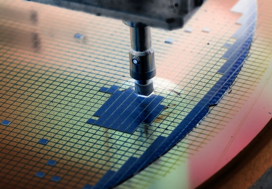
Crack inspection inside silicon wafer edge after dicing.
●Installed Product
Case Study Digest
| Challenges/Issues | "VS-THV-SWIR" Evaluation |
|---|---|
Defects inside silicon wafers can lead to serious incidents. |
Silicon wafers have the property of transmitting SWIR light, and by using SWIR light, cracks inside the wafer can be imaged by imaging from directly above. |
Challenges/Issues
Defects inside silicon wafers can lead to serious incidents.
To remove them, visible light cannot image inside of the wafer.
The need is removing it before proceeding to the next process, and save the waste.
"VS-THV-SWIR" Evaluation
Silicon wafers have the property of transmitting SWIR light, and by using SWIR light, cracks inside the wafer can be imaged by imaging from directly above.
VS-THV-SWIR contributes to image with approximately four times the transmittance at wavelengths of 1000 to 1600nm compared to visible light lenses. *Transmittance varies depending on the wavelength used.
It is compatible with SWIR light and has a lineup of high-magnification optical magnifications from 1.0 to 4.0x, so it’s able to support precision inspections of wafers in units of microns.
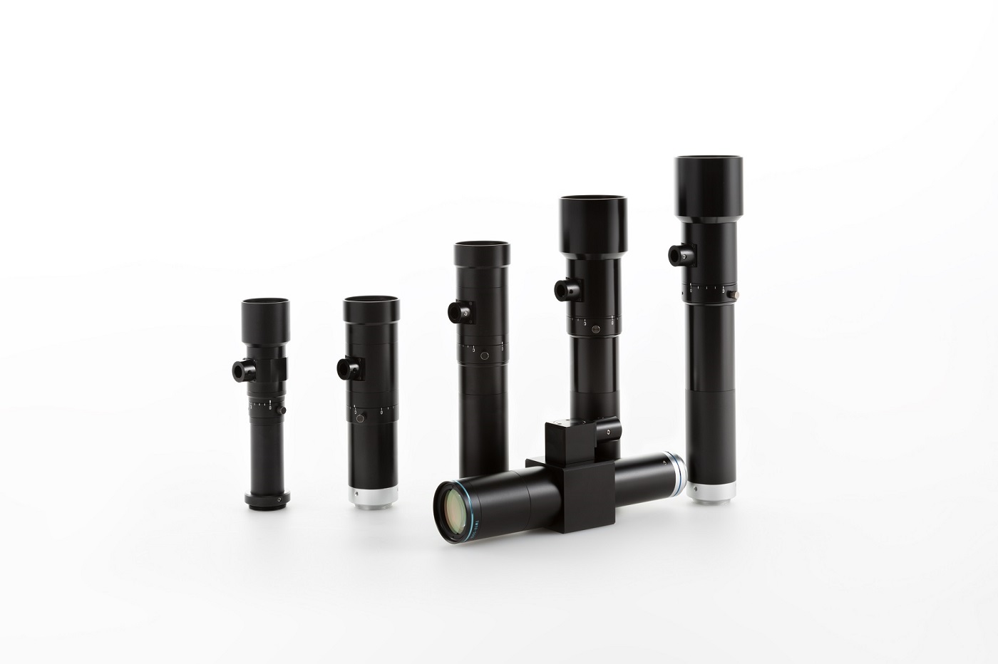
| About the "VS-THV-SWIR" series selected to solve the issue in the case study. | |
|---|---|
 |
1″ and 1.1″ Support Telecentric Lenses |
About the "VS-THV-SWIR" series selected to solve the issue in the case study.
1″ and 1.1″ Support Telecentric Lenses
・Optical Mag. 1.0x/1.5x/2.0x/3.0x/4.0x
・1.0x, 1.5x, and 2.0x are 1″ support、3.0 and 4.0x are 1.1″ support
・Lens with enchanced transmittance from 1000nm to 1600nm
・Adjustable DOF for all models with variable aperture
Related Product
-
- NIR / SWIR
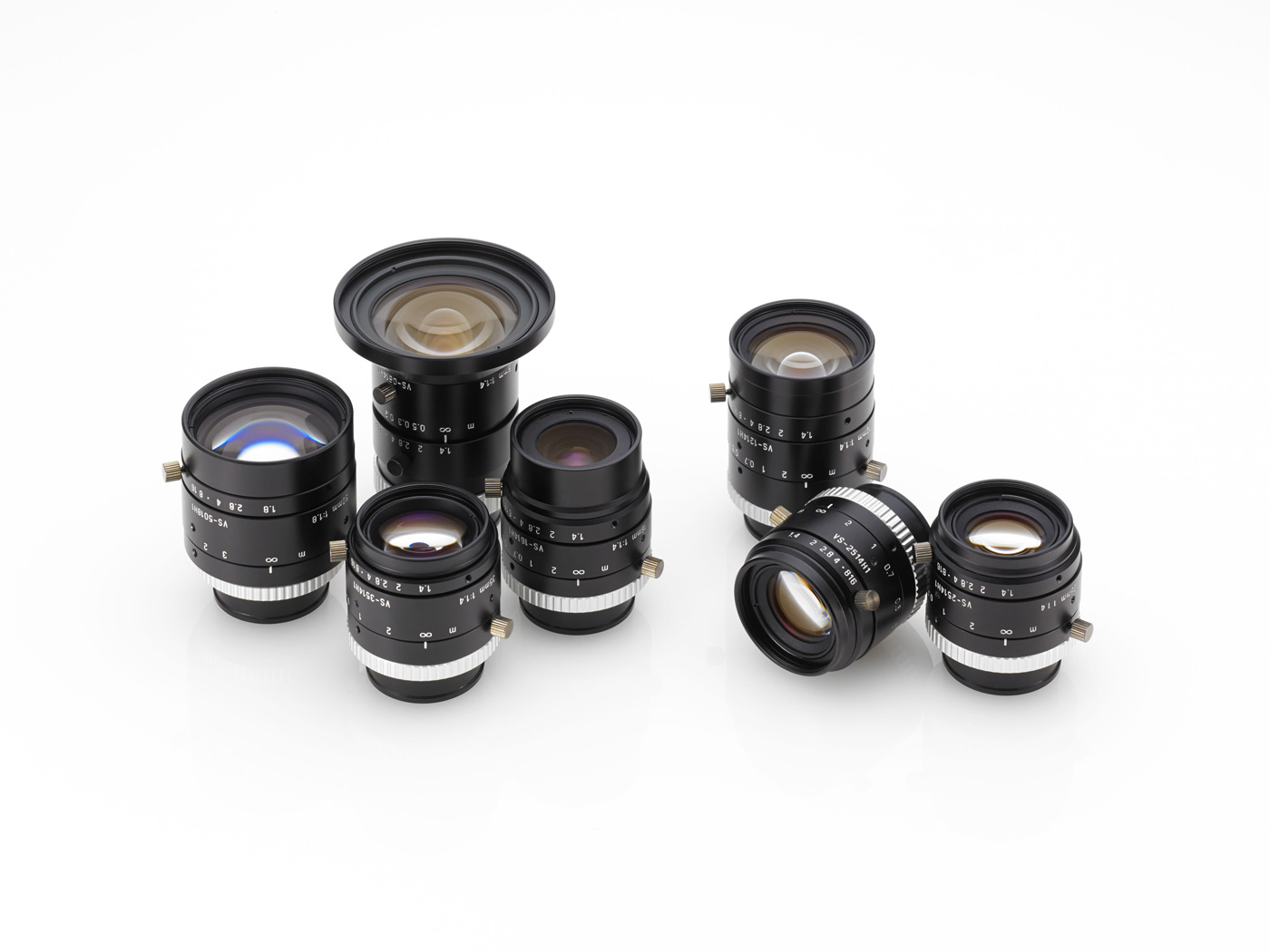
VS-H1-SWIR Series
 Specifications, Drawings
 -
- NIR / SWIR
VS-TM-SWIR Series
 Specifications, Drawings
