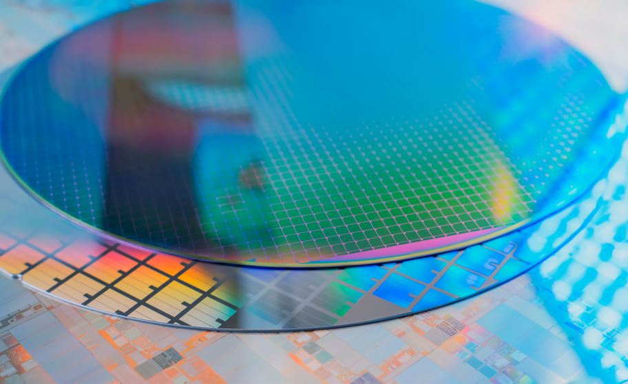
Inspection of Silicon Wafer
What is the lens selected to improve the accuracy of inspection for abnormalities and foreign particles in patterned circuits on silicon wafers?
●Installed Product
Case Study Digest
| Challenges/Issues | VS-THV-SWIR Evaluation |
|---|---|
・Customer request for higher resolution and inspection accuracy |
・The SWIR-compatible high-resolution lens can handle the latest high-resolution sensors and improve resolution. |
Challenges/Issues
・Customer request for higher resolution and inspection accuracy
・Additional request to increase takt time by enlarging the imaging area.
VS-THV-SWIR Evaluation
・The SWIR-compatible high-resolution lens can handle the latest high-resolution sensors and improve resolution.
・The high transmittance of the SWIR and the ability to capture images brightly led to an improvement in tact time.
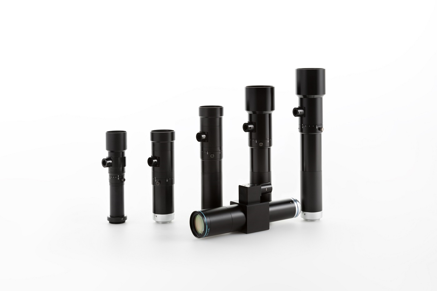
| About the VS-THV-SWIR series selected to solve the issue in the case study. | |
|---|---|
 |
See What is Hidden ・SWIR optimized coaxial light input port |
About the VS-THV-SWIR series selected to solve the issue in the case study.
See What is Hidden
Telecentric Lenses for 1000nm ~ 1600nm SWIR
・SWIR optimized coaxial light input port
・1.1” & 1” support
・Optical mag. 1.0x/1.5x/2.0x/3.0x/4.0x, 5 models
・Co-axial lighting
Related Product
-
- NIR/SWIR
VS-H1-SWIR Series
 Specifications, Drawings